
What Is TVS Surge Protection and How Does It Work?
Electronic devices rarely fail because of one dramatic event. More often, a brief voltage spike quietly weakens sensitive components. A nearby lightning strike, inductive motor, or faulty power switch can create sudden electrical stress. Tvs Surge Protection helps limit that threat before it reaches vulnerable circuits.
A transient voltage suppressor, or TVS diode, normally behaves like a high-resistance component. When voltage remains within a safe range, it stays largely inactive. During a surge, its resistance drops sharply. It then diverts excessive current toward ground or another designated return path. This response can occur within nanoseconds. It may protect microcontrollers, communication ports, sensors, and power rails. The device does not remove electricity. It clamps the voltage to a safer level.
Real protection depends on correct selection and physical layout. Engineers compare standoff voltage, breakdown voltage, clamping voltage, peak pulse power, and surge duration. A diode rated too low may conduct during normal operation. One rated too high may clamp above the circuit’s safe limit. Short traces, suitable grounding, and careful placement matter too. A perfect datasheet choice can still perform poorly on a crowded board.
That point deserves attention. TVS protection is not a universal shield. Repeated surges, heat, poor grounding, and incorrect ratings can reduce its effectiveness. Even experienced designers sometimes overlook board-level details. This guide explains how Tvs Surge Protection works, where it fits, and which practical decisions require closer review before production.
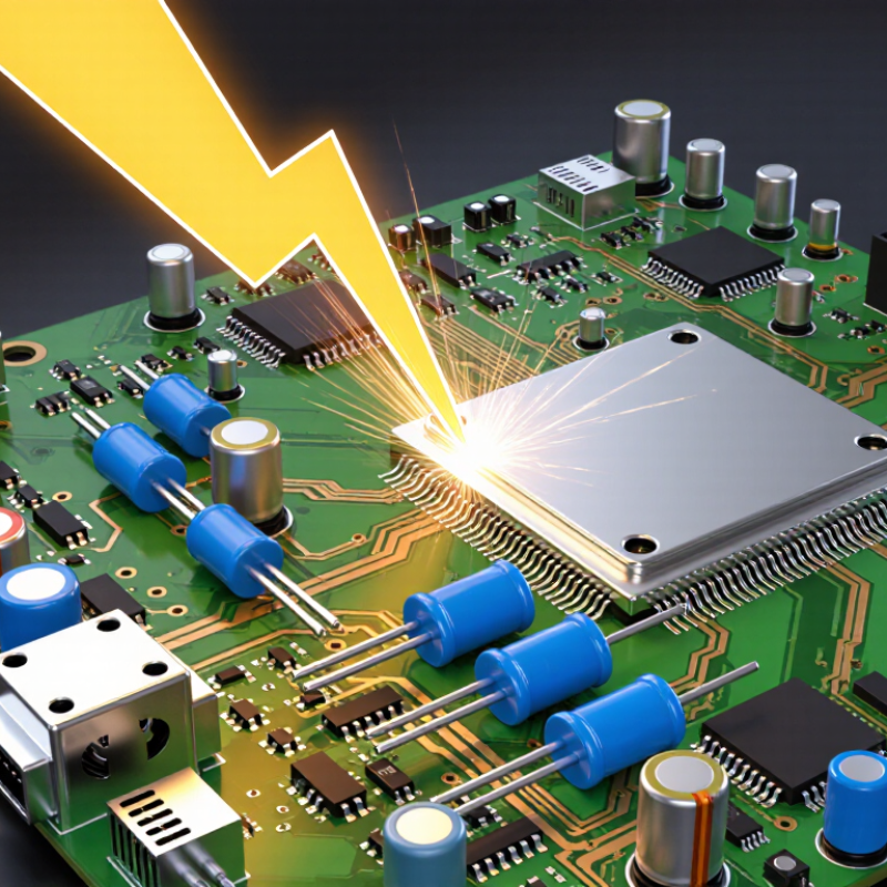
TVS Diodes Defined: The PN-Junction Device Behind Surge Protection
A transient voltage suppression (TVS) diode is a PN-junction device designed to react to sudden voltage surges. Its junction contains a depletion region that normally blocks reverse current. When voltage exceeds its breakdown level, the electric field becomes strong enough to trigger avalanche multiplication. Current then rises sharply through the diode, limiting the voltage seen by sensitive components.
That action is extremely fast. During a surge, the TVS diode provides a low-impedance path to ground or another return node. The protected circuit receives a clamped voltage instead of the full transient. A unidirectional diode behaves like a conventional diode in forward bias, while a bidirectional type handles positive and negative excursions similarly. The selected standoff voltage must remain above the circuit’s highest normal voltage. Otherwise, unwanted leakage or heating may occur.
Practical testing reveals details that simplified diagrams hide. A diode’s clamping voltage depends on pulse current, temperature, and dynamic resistance. PCB trace inductance also matters. The shorter the path, the better. A long ground connection can weaken protection, even with a suitable device. Engineers should compare the expected surge waveform with the diode’s rated pulse power and response data. Do not trust one number alone. Datasheet ratings often use controlled conditions, while real boards contain tolerances, connectors, and imperfect grounding. That gap deserves careful review.
What Is TVS Surge Protection and How Does It Work? — TVS Diodes Defined: The PN-Junction Device Behind Surge Protection
| Technical Dimension | What It Means | Typical Engineering Information | Design and Protection Notes |
|---|---|---|---|
| Basic Device Type | A Transient Voltage Suppressor (TVS) diode is a semiconductor device designed to limit short-duration voltage surges. | Silicon PN-junction device | It remains mostly non-conductive during normal operation and conducts heavily when the transient voltage reaches its breakdown region. |
| Primary Function | Divert excessive transient current away from sensitive circuitry and restrict the voltage across the protected node. | Voltage clamping through avalanche breakdown | A TVS diode does not eliminate surge energy; it redirects and absorbs or dissipates part of it within the limits of its rated pulse capability. |
| Normal Stand-Off Voltage (VRWM) | The maximum continuous reverse voltage that can be applied without significant conduction. | Selected to be equal to or slightly higher than the normal maximum circuit voltage | Choosing a stand-off voltage that is too low can cause unwanted leakage or heating during normal operation. |
| Breakdown Voltage (VBR) | The voltage range where avalanche conduction begins under a specified test current. | Typically higher than VRWM and lower than the specified clamping voltage | Breakdown voltage is not the same as the final voltage seen by the protected circuit during a high-current surge. |
| Clamping Voltage (VC) | The maximum measured voltage across the TVS diode during a defined peak pulse current. | Often specified using an 8/20 μs surge waveform | The protected component must have a safe operating voltage higher than the actual clamping voltage, including layout and wiring inductance. |
| Peak Pulse Current (IPP) | The maximum peak current the device can conduct for a specified transient waveform and duration. | Common ratings range from several amperes to hundreds of amperes, depending on package and waveform | The current rating is meaningful only when the test waveform, pulse duration, repetition rate, and initial temperature are also considered. |
| Response Time | The time required for the device to begin responding to a rapid voltage transient. | The semiconductor junction response is commonly in the sub-nanosecond to nanosecond range | PCB trace length, package inductance, and connection geometry can create additional voltage overshoot before the TVS diode conducts effectively. |
| Unidirectional TVS | Conducts like a rectifier diode in the forward direction and provides avalanche protection in the reverse direction. | Typically used on DC power rails and circuits with a defined polarity | It can provide a low forward-voltage path for transients with the opposite polarity. |
| Bidirectional TVS | Provides similar avalanche protection for positive and negative voltage transients. | Commonly used on AC lines, differential interfaces, and signal pairs | It is useful where the protected signal routinely swings in both voltage directions. |
| Junction Capacitance | The diode capacitance that can load or slow a high-speed signal. | May range from less than 1 pF for low-capacitance signal protection to tens or hundreds of pF for power protection | Low-capacitance devices are preferred for high-speed data lines, while power rails can generally tolerate higher capacitance. |
| Leakage Current | The small current that flows when the applied voltage is below the breakdown region. | Usually specified at VRWM; values range from nanoamperes to microamperes depending on device design | Low leakage is important in battery-powered equipment and high-impedance measurement circuits. |
| Energy Handling | The ability to withstand and dissipate transient energy without thermal or junction damage. | Specified in joules or through a defined peak pulse power rating, commonly measured for a 10/1000 μs waveform | A short, high-current pulse and a longer, lower-current pulse can impose very different thermal stresses. |
| Typical Surge Sources | Events that create a rapid rise in voltage or current on a circuit. | Electrostatic discharge, inductive switching, cable coupling, automotive load dump, and lightning-induced transients | The TVS rating and test waveform should be selected to match the expected environment rather than a generic surge label. |
| Recommended PCB Placement | The physical location and routing used to connect the TVS diode to the protected circuit. | As close as practical to the connector or surge entry point | Use short, wide traces and a low-inductance return path. Avoid routing surge current through sensitive component ground paths. |
| Failure Mode | A TVS diode may fail when a transient exceeds its thermal, current, or energy limits. | Often fails short-circuit after severe overstress, although failure behavior depends on construction and application | A properly selected fuse, current limiter, or upstream protection device may be required to prevent sustained fault heating. |
Note: Electrical values are representative engineering ranges. Always verify the exact voltage, current, waveform, temperature, capacitance, and package ratings for the intended circuit.